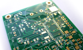
Double Sided Circuits
Double Sided Circuits
Double sided printed circuit boards are the most widely used of the PCB family. They consist of two (“double”) conductive layers and one layer of solder mask insulating layer on the top and bottom. Standard overall thicknesses range from .031” ‐ .125”. This makes them useful for most electronic applications such as control boards and user interface boards. All component types can be attached to double sided circuits and current carrying capabilities of signal traces range from a few milliamps to several amps.
Some Key Points
- Simple and robust construction well suited for most electronic applications
- Solid rigid construction able to endure years of operation without failure
- Wide operating temperature range up to 255°C depending on the materials used
- Mount all component types – surface mount (SMT), thru – hole, wire bond, BGA
- Meets IPC‐6012 Qualifications and Performance Specifications for Rigid Printed Boards
Design Capabilities
- Layer Count: 2 conductive layers
- Trace/Space: .003”/.003” typical, .002”/.002” non‐typical
- Current Carrying Capacity: few milliamps to several amps
- Hole Size: .006” drilled not plated and .008” drilled plated typical
- Copper Thickness: ½ oz, 1 oz, 2 oz typical, 3oz, 4oz non‐typical
- Material thickness: .031”, .062”, .093” and .125” typical


