Reverse Bared Circuits
Reverse Bared Circuits
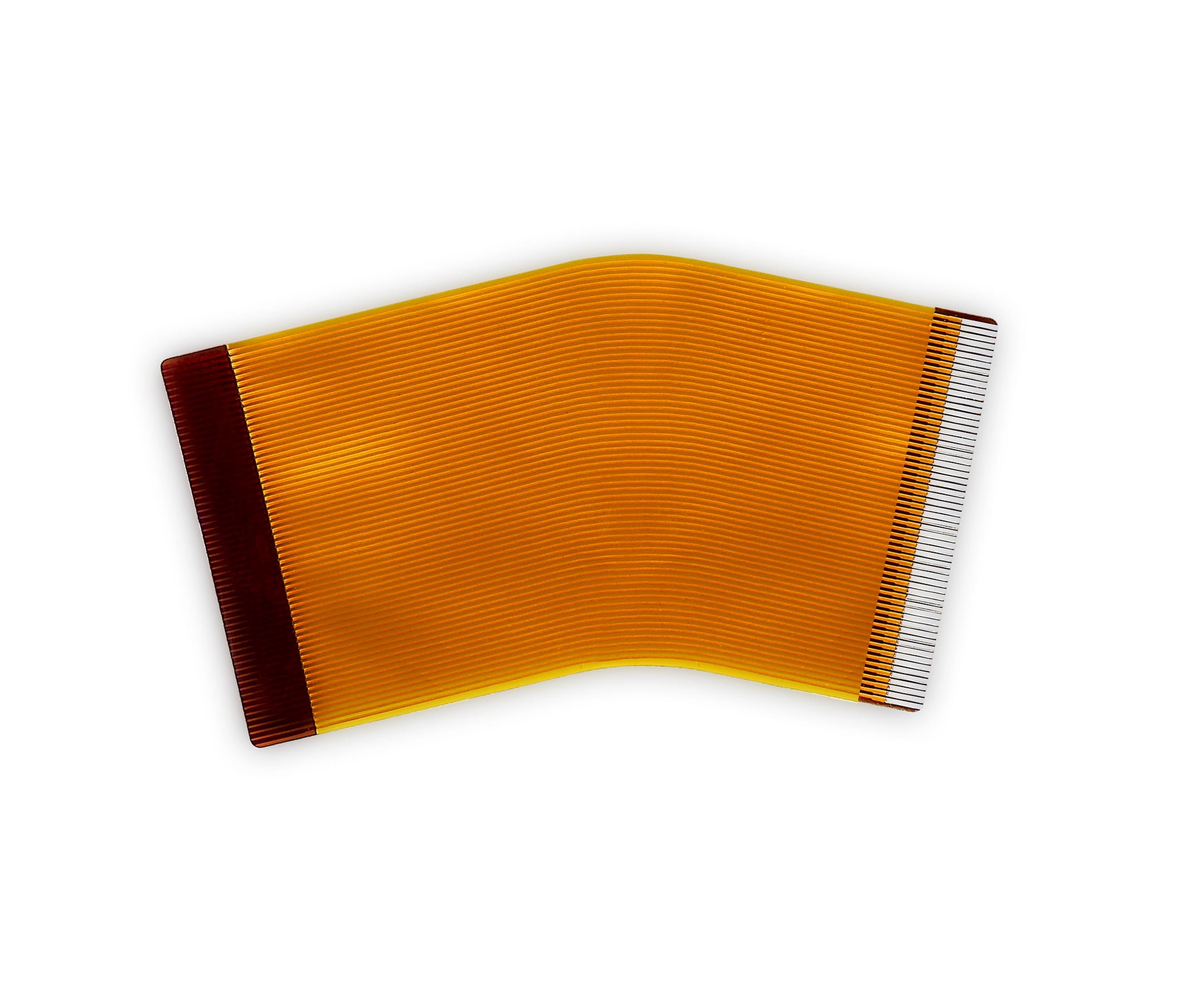
Reverse bared flexible circuits are also a unique member of the flexible circuit family. They consist of a “single” conductive layer and two insulating layers very much like a single sided circuit. The unique difference is that the base material layer is cut out to allow exposed traces/pads on both sides similar to a double sided circuit. This allows us to create circuits with connector pads on both sides which eliminate the need to twist the circuit. Also, this construction allows component attachment on both sides for applications such as backlight panels. These circuits are the thinnest of the flexible circuit family with an overall thickness range of 3.7 (.0037”) to 5.4 (.0054”) mils typically. All component types can be attached to reverse bared circuits and current carrying capabilities of signal traces range from a few milliamps to several amps.
Some Key Points
- More complex than typical single sided circuits, but less cost than double sided circuits
- Thin and light weight, yet durable enough for any application
- Wide operating temperature range from ‐55°C ‐ 150°C
- Mount all component types – surface mount (SMT), thru – hole, crimp on pins, wire bond, BGA
- Meets IPC‐6013 Qualifications and Performance Specifications for Flexible Printed Boards
Design Capabilities
- Layer Count: 1 conductive layer
- Connector Pitch: 0.3mm, 0.5mm, 1.0mm typical
- Hole Size: .008” drilled not plated typical, .004” laser drilled non‐typical
- Copper Thickness: ¼ oz, ½ oz, 1 oz, 2 oz typical
- Material thickness: 1 mil, 2 mil typical, 3 mil and 5 mil non‐typical
- FR4 Stiffener Thickness: .010” ‐ .125”
- Polyimide Stiffener Thickness: .002” ‐ .010”


